2026-06-08 · STM32 · ADC · DMA
STM32 ADC + DMA Scan Mode
Continuous Conversion on H723, H743 & U5
A register-level guide to configuring multi-channel ADC with DMA in scan/continuous mode. Why your buffer stays at zero, how to fix it, and what changes on STM32U5.
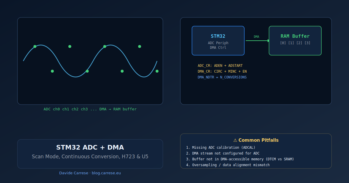
Setting up the STM32 ADC with DMA for continuous multi-channel scanning is one of the most common tasks in embedded firmware — and also one of the most common sources of frustration. The buffer stays at zero. The DMA never fires. The ADC converts once and stops.
This guide covers the register-level configuration for STM32H723, H743, and the key differences on STM32U5, based on real Stack Overflow questions with thousands of views.
The Problem
A typical scenario: you configure the ADC in scan mode with DMA, call HAL_ADC_Start_DMA(), and expect your buffer to fill with samples. Instead, the buffer stays at all zeros, or the first value is correct but the rest are garbage, or the ADC converts exactly one scan then stops.
The most common causes, in order:
- ADC calibration not performed — on H7 series,
ADCALmust be done before any conversion - DMA stream not correctly configured for the ADC — wrong stream/peripheral mapping
- Buffer in wrong memory region — on H7, DTCM RAM is NOT accessible by DMA
- DMA_NDTR set incorrectly — must account for total number of transfers
- Oversampling + data alignment mismatch — 8-bit vs 16-bit DMA width
Register-Level Configuration (H723 / H743)
Step 1: ADC Calibration
On H7 series, calibration is mandatory. Without it, the ADC returns zero or invalid values.
// 1. Enable ADC interface clock
RCC->AHB1ENR |= RCC_AHB1ENR_ADC12EN;

// 2. Wait for ADC ready, then calibrate
ADC1->CR |= ADC_CR_ADVREGEN;       // Enable voltage regulator
for (volatile int i = 0; i < 10000; i++); // Wait for regulator startup

ADC1->CR |= ADC_CR_ADCAL;          // Start calibration
while (ADC1->CR & ADC_CR_ADCAL);   // Wait for completion
Step 2: ADC Configuration (Scan Mode, Continuous)
// 3. Set resolution and scan mode
ADC1->CFGR = ADC_CFGR_CONT       // Continuous conversion
           | ADC_CFGR_DMAEN       // Enable DMA
           | ADC_CFGR_DMACFG;     // DMA requests for every conversion

// 4. Set scan sequence length (e.g., 4 channels)
ADC1->SQR1 = (4 - 1) << ADC_SQR1_L_Pos;  // L field = 3 for 4 channels

// 5. Configure channels (SQR1, SQR2, SQR3, SQR4 depending on rank)
// Rank 1: channel 5 on SQR1_SQ1
ADC1->SQR1 |= 5 << ADC_SQR1_SQ1_Pos;
// Rank 2: channel 6 on SQR1_SQ2
ADC1->SQR1 |= 6 << ADC_SQR1_SQ2_Pos;
// Rank 3: channel 7 on SQR1_SQ3
ADC1->SQR1 |= 7 << ADC_SQR1_SQ3_Pos;
// Rank 4: channel 8 on SQR1_SQ4
ADC1->SQR1 |= 8 << ADC_SQR1_SQ4_Pos;

// 6. Set sampling time (SMPR1, SMPR2)
ADC1->SMPR1 |= ADC_SMPR1_SMP0_2;  // Channel 5: 92.5 cycles

// 7. Enable ADC
ADC1->CR |= ADC_CR_ADEN;
while (!(ADC1->ISR & ADC_ISR_ADRDY));  // Wait for ready
Step 3: DMA Configuration (Circular Mode)
On STM32H7, the ADC is connected to DMA1 Stream 0 (for ADC1). Critical: the DMA buffer must be in SRAM, not DTCM!
// IMPORTANT: Place buffer in SRAM, NOT DTCM!
// DTCM (0x20000000) is NOT accessible by DMA on H7
// Use SRAM1 (0x30000000) or SRAM2 (0x30020000)
__attribute__((section(".sram")))
uint16_t adc_buffer[256];  // 256 samples x 16-bit

// Configure DMA1 Stream 0 for ADC1
DMA1_Stream0->PAR = (uint32_t)&ADC1->DR;   // Peripheral address
DMA1_Stream0->M0AR = (uint32_t)adc_buffer;    // Memory address (SRAM!)
DMA1_Stream0->NDTR = 256;                      // Number of data items

DMA1_Stream0->CR = (0 << DMA_SxCR_CHSEL_Pos)  // Channel 0 (ADC1)
                 | DMA_SxCR_MSIZE_0             // Memory size: 16-bit
                 | DMA_SxCR_PSIZE_0             // Peripheral size: 16-bit
                 | DMA_SxCR_MINC                // Increment memory
                 | DMA_SxCR_CIRC                // Circular mode
                 | DMA_SxCR_DIR_0               // Peripheral-to-memory
                 | DMA_SxCR_EN;                 // Enable stream

// Enable DMA interrupt (optional)
DMA1_Stream0->CR |= DMA_SxCR_TCIE;   // Transfer complete interrupt
NVIC_EnableIRQ(DMA1_Stream0_IRQn);
On STM32H7, the DTCM RAM region (0x20000000) is connected directly to the CPU core via a dedicated bus. DMA and other bus masters cannot access it. If you declare your ADC buffer as a regular global variable, it goes to DTCM by default. The DMA will transfer all zeros because it reads from the peripheral but cannot write to DTCM.
Fix: place the buffer explicitly in SRAM1 (0x30000000) or SRAM2 (0x30020000) using the linker section attribute or by defining the variable at a specific address.
Starting Conversions
// Start ADC conversion
ADC1->CR |= ADC_CR_ADSTART;

// Or with HAL:
// HAL_ADC_Start_DMA(&hadc1, (uint32_t*)adc_buffer, 256);
The ADC will continuously scan all 4 channels, generating a DMA request after each conversion. The DMA transfers the result to adc_buffer in circular mode. When the buffer is full (256 samples), the DMA wraps around and starts from the beginning, optionally firing an interrupt.
STM32U5 Differences
The STM32U5 series introduced a new ADC HAL that differs from the H7 in several important ways:
| Feature | H723 / H743 | STM32U5 |
|---|---|---|
| DMA trigger | DMA request per conversion | DMA transfer by burst (DFSDM-like) |
| Calibration | ADCAL bit | ADCAL + ADCALDIF for differential |
| Data register | ADC->DR single | ADC->DR + regular/ injected distinction |
| DMA config | DMA1 Stream 0 | GPDMA, linked-list descriptors |
| Oversampler | 2..256x, separate block | Integrated in ADC, hardware averaging |
| OS/alignment | Left/right alignment in CFGR | More flexible data shift registers |
The main difference on U5 is the GPDMA (general-purpose DMA) instead of the traditional STM32 DMA streams. GPDMA uses a linked-list descriptor model — each descriptor defines one transfer sequence. You build a chain of descriptors and trigger them. This is more flexible but requires more setup code.
Additionally, the U5's ADC has a different oversampling block. If you enable hardware oversampling (OSR), the data width changes: with OSR > 1, the ADC outputs right-shifted data, and the DMA transfer width must match the resulting resolution (usually 16-bit). Mismatching the DMA data width is a common source of "buffer stays at zero" on U5.
Debugging Checklist
| # | Check | Symptom if wrong |
|---|---|---|
| 1 | ADC calibration done? | Values at zero or random |
| 2 | Buffer in DMA-accessible RAM? | Buffer stays at zero (H7 DTCM) |
| 3 | DMA stream matches ADC? | DMA never fires |
| 4 | DMA_NDTR > 0? | DMA transfers 0 items |
| 5 | ADC clock enabled? | ADC stays at zero |
| 6 | ADC_CFGR_DMAEN set? | ADC doesn't request DMA |
| 7 | Sampling time long enough? | Garbage values from fast channels |
| 8 | Data alignment matches? | Values shifted or truncated |
| 9 | Oversampling + DMA width match? | U5: zeros with OSR enabled |
| 10 | PCLK < ADC max frequency? | ADC results invalid |
Putting It All Together
Here's a minimal working sequence in register-level style:
// === ADC1 init (H723) ===
RCC->AHB1ENR |= RCC_AHB1ENR_ADC12EN;
ADC1->CR |= ADC_CR_ADVREGEN;
delay_us(20);
ADC1->CR |= ADC_CR_ADCAL;
while (ADC1->CR & ADC_CR_ADCAL);

ADC1->CFGR = ADC_CFGR_CONT | ADC_CFGR_DMAEN | ADC_CFGR_DMACFG;
ADC1->SQR1 = (3 << ADC_SQR1_L_Pos) | (5 << ADC_SQR1_SQ1_Pos)
           | (6 << ADC_SQR1_SQ2_Pos) | (7 << ADC_SQR1_SQ3_Pos)
           | (8 << ADC_SQR1_SQ4_Pos);
ADC1->SMPR1 = ADC_SMPR1_SMP0_2;

ADC1->CR |= ADC_CR_ADEN;
while (!(ADC1->ISR & ADC_ISR_ADRDY));

// === DMA1 Stream 0 init ===
__attribute__((section(".sram"))) static uint16_t buf[128];

DMA1_Stream0->PAR = (uint32_t)&ADC1->DR;
DMA1_Stream0->M0AR = (uint32_t)buf;
DMA1_Stream0->NDTR = 128;
DMA1_Stream0->CR = (0 << DMA_SxCR_CHSEL_Pos) | DMA_SxCR_MSIZE_0
                 | DMA_SxCR_PSIZE_0 | DMA_SxCR_MINC | DMA_SxCR_CIRC
                 | DMA_SxCR_DIR_0 | DMA_SxCR_EN;

// === Start ===
ADC1->CR |= ADC_CR_ADSTART;
// Now buf[] fills continuously with [ch5][ch6][ch7][ch8][ch5]...
References
- SO: STM32 ADC + DMA does not update value (H723ZG)
- SO: ADC + DMA different on STM32U5
- RM0468: STM32H723 Reference Manual
- RM0456: STM32U5 Reference Manual
Davide Carrese · Embedded Firmware Engineer · carrese.eu
Comments
Have comments? Send me an email.